
PCB Design Layout Guidelines and Best Practices for Engineers
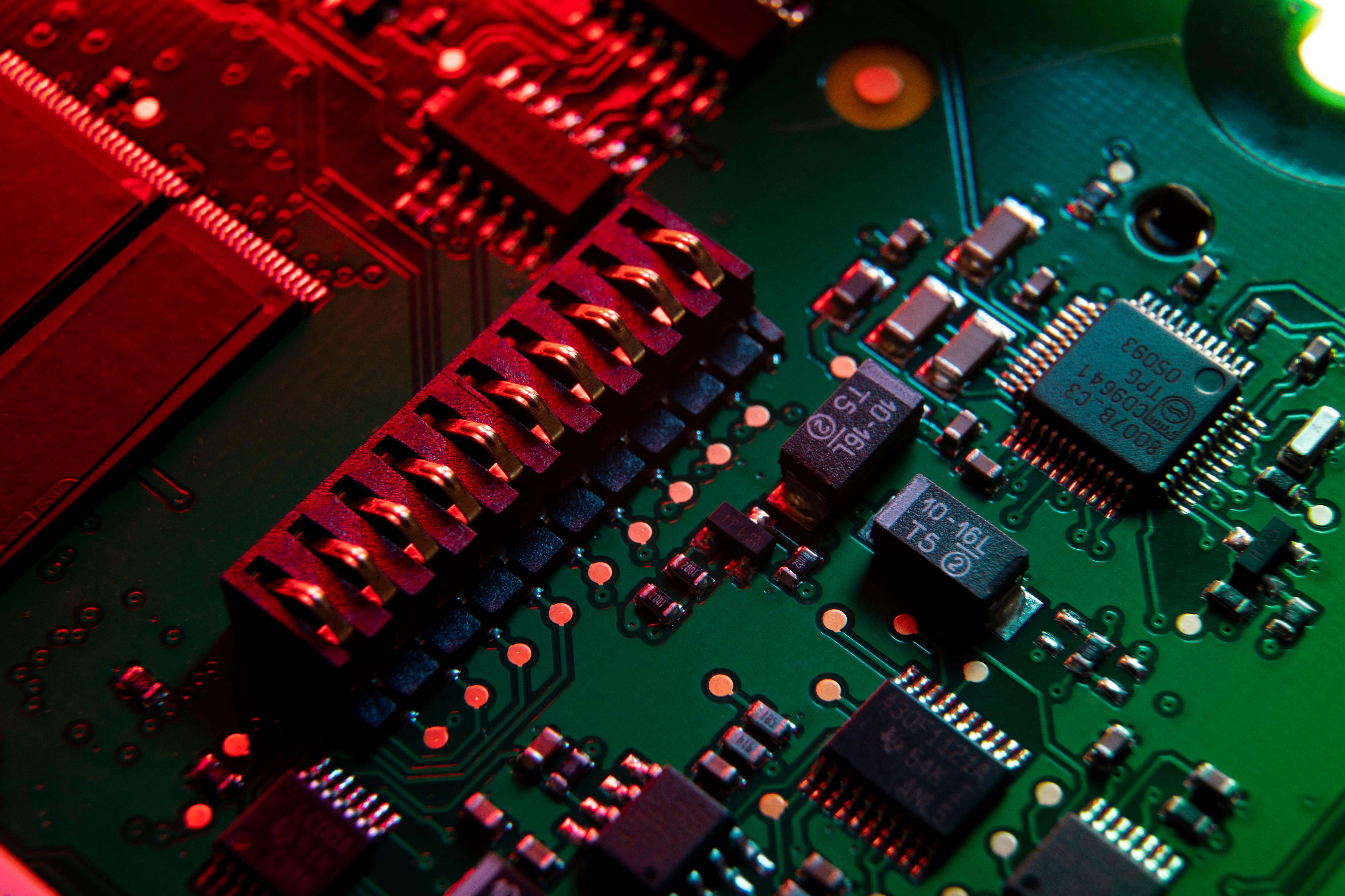
Printed Circuit Boards (PCBs) are the backbone of modern electronics, connecting components and enabling complex functionality within a compact footprint. Achieving a reliable, manufacturable, and high-performance PCB requires adherence to structured PCB layout guidelines and best practices. Whether working on consumer devices or complex industrial electronics, engineers must balance signal integrity, thermal management, manufacturability, and long-term reliability. This guide provides practical, engineering-focused strategies for PCB layout design, including component placement, PCB trace routing, power and ground management, signal integrity, EMI mitigation, design for manufacturability (DFM), and final verification. Following these principles ensures successful hardware development and high-quality end products.
Component Placement: The Foundation of PCB Layout
Proper component placement is the most critical stage of PCB layout design, as it influences routing complexity, system performance, thermal behavior, and assembly efficiency.
Best practices for component placement:
- Functional Grouping: Place components that interact frequently close together to reduce trace lengths and improve signal integrity. Keep analog circuitry separate from digital sections to minimize noise coupling, and group power-supply components to enhance thermal management.
- Signal Flow Optimization: Arrange components to follow the natural direction of the signal path. Shorter trace lengths reduce delay, resistance, and parasitic capacitance, which is critical for high-speed and high-frequency circuits.
- Testing Accessibility: Ensure test points, connectors, and programming headers remain accessible during debugging, validation, and manufacturing.
- Thermal Considerations: Place high-power components such as voltage regulators, power MOSFETs, and LEDs to allow effective heat dissipation and airflow, while keeping heat-sensitive components away from hot zones.
- Consistent Component Orientation: Align similar components uniformly to simplify assembly, reduce soldering errors, and streamline visual inspection.
Effective component placement reduces routing complexity, minimizes crosstalk, and enhances overall manufacturability.
Example: In a microcontroller-based IoT board, placing the MCU close to its supporting decoupling capacitors and voltage regulators ensures stable power delivery and helps reduce noise introduced into sensitive analog sensors.
Trace Routing: Connecting Components Efficiently
After placing components, trace routing defines the conductive paths that connect each part according to the schematic. Proper trace routing is critical for maintaining signal integrity, controlling EMI, and ensuring manufacturability.
Key PCB trace routing guidelines:
- Keep Traces Short: Shorter traces minimize resistance, inductance, capacitance, and signal delay, critical for high-speed digital circuits.
- Trace Width Considerations: According to established PCB layout rules, high-current traces should be wider to prevent overheating, while controlled-impedance signals, such as USB or Ethernet, require precise trace widths.
- Avoid 90-Degree Angles: Use 45-degree or curved traces to minimize signal reflections and improve manufacturability. Sharp corners can also form acid traps during etching, which may compromise board quality..
- Analog & Digital Trace Separation: Isolate noisy digital traces from sensitive analog signals to minimize interference and signal degradation.
- Separate analog and digital traces: Isolate noisy digital lines from sensitive analog signals to prevent interference.
- Use ground planes strategically: Implement a continuous ground plane to reduce EMI, provide a stable reference, and improve thermal dissipation.
- Layer Management: Use multilayer boards to separate power, ground, and signal layers, enabling cleaner routing and reducing crosstalk.
Example: In a high-speed communication PCB, differential pairs for USB or HDMI must be routed with precise spacing and matched lengths to maintain signal integrity.
Power and Ground Planning
Reliable power delivery is critical for PCB performance. Poor planning can lead to voltage drops, excessive noise, and device instability.
Key guidelines for power and ground management:
- Use dedicated power and ground planes whenever possible.
- Place decoupling capacitors close to IC power pins to filter noise.
- Route high-current traces directly from source to load to minimize resistance.
- Avoid splitting planes in critical areas, especially under sensitive analog or high-speed components.
- Consider thermal relief in power planes for heat dissipation.
Proper power and ground design ensures consistent voltage levels, reduces EMI, and improves reliability.
Signal Integrity and EMI Considerations
High-speed and sensitive circuits require careful attention to signal integrity and electromagnetic interference (EMI). Applying best practices early in the design phase prevents costly redesigns later.
Key techniques:
- Differential pair routing: Route differential pairs for high-speed signals such as USB, HDMI, and PCIe.
- Controlled impedance traces: Maintain consistent impedance for RF and high-speed digital lines.
- Proper termination and via placement: Reduce reflections, ringing, and signal degradation.
- Shielding and trace separation: Route high-speed or noisy signals away from sensitive analog circuits.
- Decoupling and bypass capacitors: Place decoupling and bypass capacitors to minimize voltage spikes and EMI across power lines.
Design for Manufacturability (DFM)
Even well-designed circuits can fail in production without manufacturability considerations. PCB design must account for assembly constraints to ensure efficient production and high yields.
Key DFM practices:
- Stress testing: Ensure adequate pad sizes and clearances to support soldering and automated assembly.
- Thermal testing: Maintain component spacing compatible with pick-and-place machines.
- Compliance testing: Avoid tight trace-to-trace or trace-to-pad clearances that exceed fabrication tolerances.
- Battery certification: Include accessible test points for in-circuit testing and debugging.
- Battery certification: Design fiducials and alignment markers to aid automated assembly.
Following these DFM rules reduces errors, speeds assembly, and minimizes production costs.
Thermal Management
Heat can significantly affect PCB performance and longevity. Engineers should integrate thermal management strategies early in layout and design.
Key thermal management practices:
- Separate high-power components to prevent hotspots.
- Use thermal vias to transfer heat from components to internal planes.
- Add copper pours and heatsinks where necessary.
- Ensure airflow paths for components that require cooling.
Effective thermal management improves reliability, prevents performance degradation, and ensures compliance with safety standards.
Final Verification and Review
Before fabrication, rigorous verification ensures the PCB is production-ready.
Key verification practices:
- Design Rule Check (DRC): Confirm trace widths, clearances, and layer rules.
- Electrical Rule Check (ERC): Validate connectivity, power distribution, and signal paths.
- Simulation: Use signal integrity, thermal, and EMI analysis to uncover hidden issues.
- Peer review: Fresh eyes on the design help catch overlooked mistakes and improve adherence to best practices.
Proper verification reduces costly revisions and ensures a robust, high-performance PCB.
Advanced PCB Design Considerations
For complex or high-performance boards, additional design practices help optimize performance and manufacturability.
Key advanced design practices:
- High-speed differential pairs: Match lengths and maintain consistent impedance for USB, PCIe, or HDMI signals.
- RF board design: Integrate shielding, controlled impedance, and tuned antennas.
- Multi-layer stackup: Optimize layer ordering for power, ground, and signal layers to minimize EMI.
- Blind and buried vias: Reduce board size and improve routing density for advanced PCBs.
- Embedded components: Reduce board area and improve signal integrity in highly compact designs.
These advanced practices are essential for modern electronics, including smartphones, IoT devices, and industrial automation boards.
Conclusion
Successful PCB development requires a structured approach based on sound engineering principles and adherence to established PCB layout guidelines. By applying best practices for component placement trace, PCB trace routing, power integrity, signal control, EMI mitigation, and manufacturability, designers can produce reliable, high-performance electronics that scale from prototype to mass production.
Mastering these PCB layout rules and practices enables engineering teams to deliver products that meet performance, reliability, and market expectations.